SCANNING ELECTRON MICROSCOPY IN MATERIALS SCIENCE
-
Days
From 12 December 2017 To 15 December 2017
-
Address
CNR IMM Bologna, Via Gobetti 101, 40129 - Bologna, Italy
-
SOLDOUT
events content
Price bundles
-
FULL REGISTRATION Members : €300.00 Non-Members :€ 400.00
Full registration
-
STUDENT REGISTRATION Members : €210.00 Non-Members :€ 280.00
Student registration


Contatti evento:
Phone :
2018-2019 Pier Giorgio Merli (S)TEM SCHOOL IN MATERIALS SCIENCE
-
Days
From 19 November 2018 To 23 November 2018
From 4 February 2019 To 8 February 2019
-
Address
CNR - IMM Sezione di Bologna
Area della Ricerca
Via P. Gobetti 101, 40129 Bologna, Italy -
SOLDOUT
events content
The first theoretical part of the School (November 19-23, 2018) will start with a presentation of the elements of electron optics needed to introduce the TEM/STEM working principles and will continue with a comprehensive lesson on radiation damage to warn the students of the downsides and the possible artefacts of these powerful investigation techniques. Some essential aspects of the theory of the electron diffraction will then be used to describe the elastic interaction of the electron beam with the crystalline sample and the electron microscopy techniques that immediately follow: Selected Area and Convergent Beam Electron Diffraction (SAED and CBED). Examples of their application for crystallographic phases identification and strain determination will be illustrated. Basic crystallography notions will be also recalled in a specific lesson. The contrast mechanisms in TEM and STEM (diffraction, phase and mass-thickness) will be successively presented for their importance in studies of lattice defects, nanoparticles and nanotubes in solids and devices. In recent year, TEM/STEM imaging techniques have attained atomic resolution for all the materials of interest in materials science. In our course, a unique theory of image formation will be used to describe both the coherent (HREM) and incoherent (HAADF-STEM) approach to these high resolution techniques. The main aspects of the inelastic interaction of the electron beam with the sample will be presented to describe the two essential analytical techniques for compositional analysis: EDS and EELS. Finally, electron holography and interferometric methods will be introduced to show either the possibility to record the phase of the electron wave and to determine electric potential variations inside the samples or as alternative techniques in phase analysis and strain determination.
In the second week (February 4-8, 2019), what learnt during the first half of the school will be put into practice. Students, under teacher’s supervision, will be allowed to directly operate on the 200 kV Schottky FEG TEM-STEM (FEI Tecnai F20 ST) installed at the CNR-IMM Institute. During this week, students will be also trained to the use of some of the available simulation and data processing software essential for TEM/STEM work. Selected presentations of new products by representatives of TEM/STEM manufacturers, sample preparation instruments and accessories for electron microscopy are also planned.
At the end of the School a certificate of attendance will be given to all the participants and upon request a certificate of the acquired skills, that may be also used for obtaining academic credits, may be issued after passing a written examination.
As participation to the School is open to people from all countries the official language is English.
Important notice: participants may choose to attend either the whole course or the theoretical part only (it is not possible to register for the practical course only). As to the practical course, to guarantee enough operating time to all the students, the maximum number of participants is limited to 10. The School will take place only if a minimum number of 6 registrations to both the theoretical and practical courses will be reached.
Price bundles
-
THEORETICAL AND PRACTICAL Members : €1360.00 Non-Members :€ 1700.00
Full course
-
THEORETICAL AND PRACTICAL - STUDENT Members : €952.00 Non-Members :€ 1190.00
Full course at reduced price for students
-
THEORETICAL PART Members : €560.00 Non-Members :€ 700.00
Theoretical course only
-
THEORETICAL PART - STUDENTS Members : €392.00 Non-Members :€ 490.00
Theoretical course only at reduced price for students
Contatti evento:
Phone :
SEM School In Materials Science
-
Days
From 9 April 2019 To 12 April 2019
-
Address
CNR IOM Area Science Park Trieste, Italy
-
SOLDOUT
events content
Price bundles
-
REGULAR Members : €300.00 Non-Members :€ 400.00
Standard registration
-
STUDENT Members : €210.00 Non-Members :€ 280.00
Student and temporay staff registration

Contatti evento:
Phone :
Aldo Armigliato SEM School in Materials Science
-
Days
From 9 November 2020 To 13 November 2020
-
Address
CNR - Institute for Microelectronics and Microsystems
Bologna Research Area
via P. Gobetti 101
40129 Bologna
Italy -
SOLDOUT
events content
È rivolta a ricercatori, tecnici e studenti che intendano acquisire le competenze necessarie per il corretto utilizzo della microscopia elettronica a scansione (SEM), delle tecniche analitiche ad essa correlate e dei fasci ionici focalizzati (FIB) per lo studio e la caratterizzazione dei materiali.
La scuola prevede sia lezioni teoriche che sessioni pratiche.
A causa delle restrioni imposte dalla epidemia COVID, la scuola avrà luogo solo in modalità on-line.
Verranno organizzate sessioni in modalità remota per tutti i partecipanti sia per la parte teorica che per la parte pratica.
Price bundles
-
CORSO COMPLETO (sold out) Members : €300.00 Non-Members :€ 400.00
Corso completo (teoria e pratica)
-
CORSO COMPLETO STUDENTI(sold out) Members : €210.00 Non-Members :€ 280.00
Corso completo per studenti, PhD, pers. non strutturato
-
CORSO TEORICO(sold out) Members : €150.00 Non-Members :€ 200.00
Solo parte teorica
-
CORSO TEORICO STUDENTI(sold out) Members : €105.00 Non-Members :€ 140.00
Solo parte teorica per studenti, PhD, pers. non strutturato
-
CORSO COMPLETO ON-LINE Members : €100.00 Non-Members :€ 100.00
Corso completo on-line COVID
Contatti evento:
Phone :
Pier Giorgio Merli (S)TEM SCHOOL IN MATERIALS SCIENCE - 8th Edition
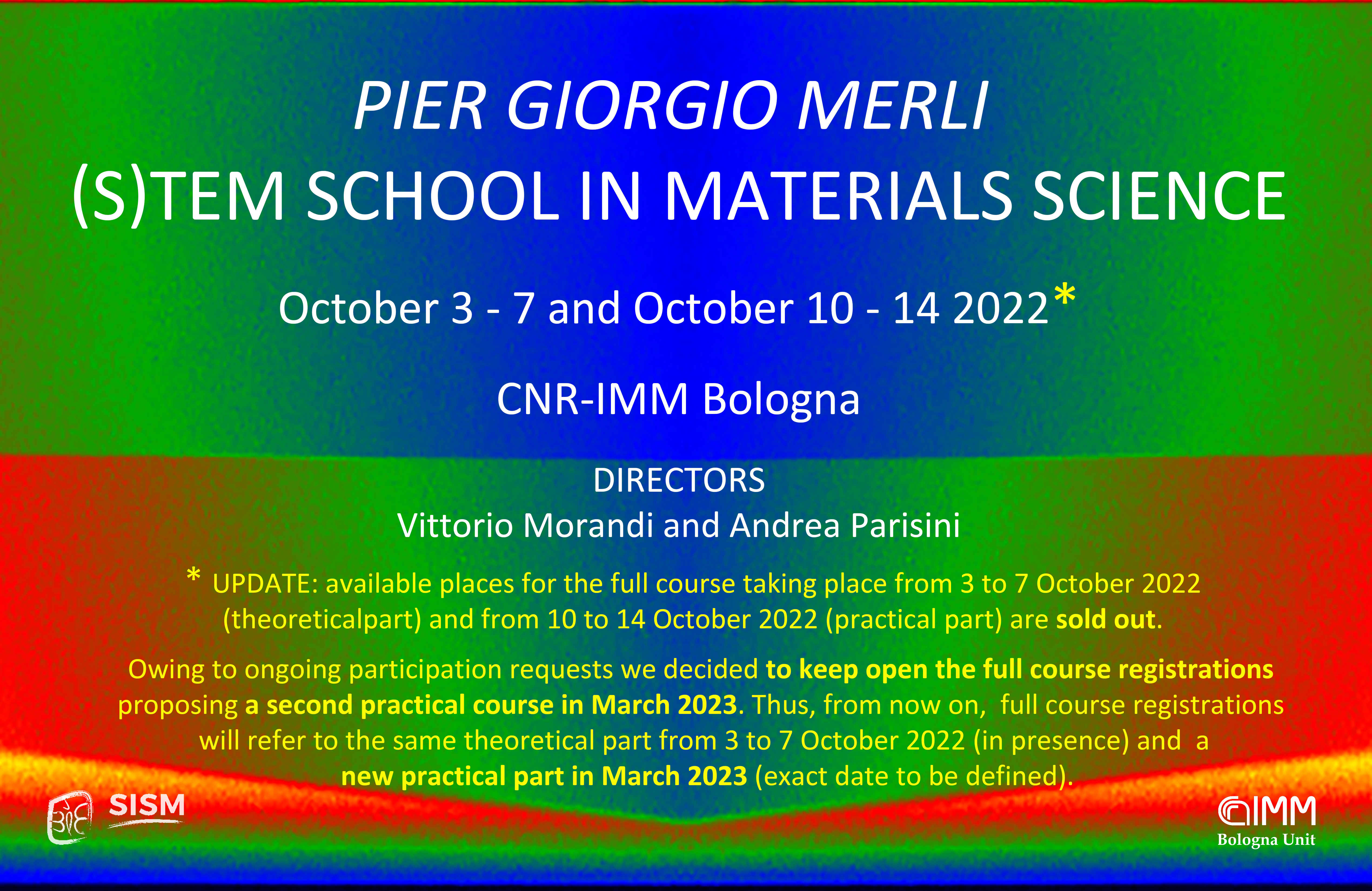
-
Days
From 3 October 2022 To 7 October 2022
From 10 October 2022 To 14 October 2022
-
Address
CNR - IMM Sezione di Bologna
Area della Ricerca
Via P. Gobetti 101, 40129 Bologna, Italy -
SOLDOUT
events content
SCHOOL REGISTRATIONS ARE OPEN, PLACES ARE AVAILABLE FOR BOTH FULL COURSE (THEORETICAL + PRACTICAL PARTS) AND THEORETICAL PART (IN-PERSON OR VIRTUAL).
Price bundles
-
FULL COURSE THEORETICAL AND PRACTICAL SESSIONS Members : €1450.00 Non-Members :€ 1500.00
Researcher
-
FULL COURSE THEORETICAL AND PRACTICAL SESSIONS Members : €950.00 Non-Members :€ 1000.00
Young scientist
-
THEORETICAL SESSION (IN PRESENCE) Members : €600.00 Non-Members :€ 650.00
Researcher
-
THEORETICAL SESSION (IN PRESENCE) Members : €400.00 Non-Members :€ 450.00
Young scientist
-
THEORETICAL SESSION (VIRTUAL) Members : €400.00 Non-Members :€ 450.00
Researcher/Young scientist
Contatti evento:
Phone :
Aldo Armigliato SEM School in Materials Science - 2023 edition
-
Days
From 11 December 2023 To 14 December 2023
-
Address
Institute for Microelectronics and Microsystems, Bologna Section,
Bologna Research Area,
Via Gobetti 101 40129, Bologna, Italy -
Closed
events content
The official language will be English.
Participation to the School will be allowed up to a maximum of 24 participants. A minimum number of 10 attendees is required to activate the School.
The school is open to SISM and EMS members. Non members are also welcomed to the School and will be requested to apply for a temporary membership during the registration process. Please follow the instruction in the registration page.
Price bundles
-
FULL COURSE Members : €350.00 Non-Members :€ 400.00
Theoretical/practical course
-
FULL COURSE FOR STUDENTS Members : €320.00 Non-Members :€ 320.00
Theoretical/practical course for students
Contatti evento:
Phone :