ELECTRON MICROSCOPY School
12-June-2019
In the Framework of Nanoinnovation 2019, University La Sapienza, NanoItaly, AIRI and SISM organize the Electron Microscopy School "Bridging organic and inorganic electron microscopy methods"
The recent achievements of transmission electron microscopy, with particular attention to the cryo-microscopy aspects are illustrated by recognized experts in the field. The school, structured also for non-specialists, illustrates the basis of Transmission Electron Microscopy either in material science and in life sciences, describes the main methods providing information at atomic level both on hard and soft matter together with the main sample requirement and the relative preparation methods.
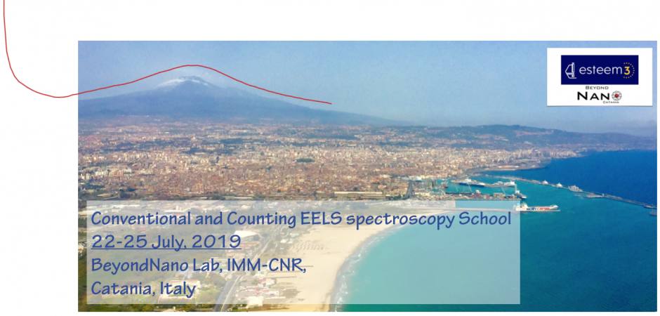
Conventional and Counting EELS spectroscopy school
01-June-2019
The Conventional and Counting EELS spectrocopy school is an intensive 4-day training school that incorporates lectures, computer laboratories, and microscope practicals to provide participants with comprehensive, hands-on training on key EELS topics and technology. The practical lessons will be made at the new Beyond-Nano Sub-Ångstom Lab on integrated JEOL GIF/EELS systems. Thanks to the Transmission electron microscopy (TEM) nowadays we can reveals details of natural and man-made structures even at sub-nanometer scale. Electron energy-loss spectroscopy (EELS) is the ideal analytical tools to the high spatial resolution provided by TEM in both the conventional and scanned (STEM) imaging modes.
PhD School at Università di Genova
11-June-2019
These are the last few days for applying for an exciting Microscopy PhD program at Diaspro Lab - deadline June 12th - for motivated future researchers.
Please, consider the following research programs:
https://www.iit.it/phd-school-docs/phd-2019/684-phd-themes-35-bionanoscienze/file
and check on the institutional websites the application modalities.
Bando Premi SISM 2019
10-January-2019
la Società Italiana Scienze Microscopiche, in collaborazione con le Aziende del settore della Microscopia, bandisce
10 premi dell’importo di 500,00 euro ciascuno, per favorire la partecipazione di ricercatori al MCM2019 (https://www.sdm.edu.rs/mcm2019/) che si terrà in Serbia a Belgrado, dal 15 al 20 settembre 2019. I Premi sono riservati a ricercatori non strutturati.
La scadenza del bando è il 1 giugno 2019.
![]()
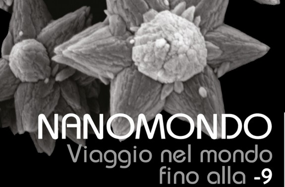
NANOMONDO - Viaggio nel mondo fino alla -9
27-October-2018
It is well known the existence of a world much larger than that on human scale,
populated by planets, stars, black holes, etc. and we know how to observe it:
through a telescope but, is there also an infinitely small world? Yes, it exists and
we can observe it! How? Through an electron microscope. The exhibition is
designed to give the opportunity to know the "nanoworld". The visitor feels like
a researcher who observes, between curiosity and amazement, real images of
nature and man-made technology. What we are proposing is an exhibition of
images of micro and nanometric structures obtained through a scanning
electron microscope (SEM) completed by dimensional scale and their magnifications.
The exhibited images, which also have a strong aesthetic value, are
accompanied by technical-scientific information, three-dimensional models
and interactive exhibits.
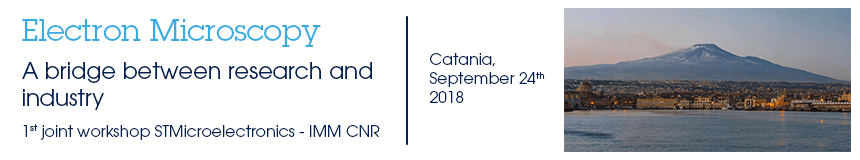
Electron Microscopy: A bridge between Reserarch and Industry
24-September-2018
The workshop is jointly organized by STMicroelectronics and the Institute for Microelectronics and Microsystems of the Italian National Research Council (IMM-CNR). It represents a melting point between the academic and research world and the industrial development in the field of the structural characterization and the microanalysis by electron microscopy.
The scope of the event will be focused on new methods applied to semiconductor devices (silicon based, wide band gap, metallic interconnections, nanotechnology, etc) and materials science. It will highlight recent progress in instrumentation, in chemical and structural analysis, in sample preparation by mechanical thinning and by FIB, as well as in situ devices polarization dependent analyses.
The scientific program will be opened by a lectio magistralis delivered by Prof. Giulio Pozzi (Department of Physics and Astronomy, University of Bologna and Ernst Ruska-Centre and Peter Grünberg Institute, Forschungszentrum Jülich) regarding Electron Holography: from the beginning to recent developments. The session will continue with scientific presentations given by researchers coming from STMicroelectronics, IMM-CNR, ENEA, LETI CEA, Cemes CNRS and Companies specialized in electron microscopy.
The workshop will present new insights focusing on the following topics:
TEM: Advanced Structural Characterization (STEM, nBED, Holodark, Tomography, ASTAR, …) and related Spectroscopic Techniques (EELS, EDS)
SEM: Advanced Characterization (EBIC, Voltage Contrast, EDS, …)
Novel specimen preparation techniques by FIB
Materials: SiC, Phase Change Materials, Metal Alloys, nanowire, ...
Latest company products: Helium Ion Microscope, New generation of (S)TEM and FIB, Highly controlled mechanical specimen preparation,..